silicon nanowires

A simple route to annihilate defects in silicon nanowires
Ngày tải lên :
16/03/2014, 15:03
... morphology of the
annealed nanowires is shown in Fig. 1. From this
image, most of the nanowires can be seen to con-
sist of straight and smoothly curved parts. The
diameters of the nanowires are around ... of silicon with a dia-
mond structure. Analysis using energy dispersive
X-ray spectroscopy (EDS) attached to the TEM
con®rmed that the nanowires have a crystalline Si
core and an amorphous silicon ... Kowloon, Hong Kong
Received 14 April 2000
Abstract
Defects inside silicon nanowires (SiNW) could be signi®cantly reduced by annealing the nanowires at 1100° C for 6
h. High-resolution transmission electron...
- 4
- 293
- 2

Carbon assisted synthesis of silicon nanowires
Ngày tải lên :
16/03/2014, 15:04
... 2003
Abstract
Carbon-assisted synthesis of silicon nanowires has been accomplished with silicon powders as well as solid sub-
strates. The method involves heating an intimate mixture of silicon powder and activated ... product. These
nanowires have diameters ranging from 50 to 700
nm, with several tens of microns in length. A low-
magnification TEM image of the nanowires is
shown in Fig. 3c. The nanowires are ... species is
generated by other means.
4. Conclusions
SiNWs have been obtained by reacting silicon
powder or silicon substrates with carbon in an
inert atmosphere. Carbothermal reduction of the
silica...
- 5
- 425
- 2

Growth kinetics of silicon nanowires by platinum assisted vapour–liquid–solid mechanism
Ngày tải lên :
16/03/2014, 15:05
... using
Fig. 1. Synthesis of Si nanowires using Au and Pt as catalysts. (a) Vertically-aligned Si nanowires using Au. (b) Vertically-aligned Si nanowires using Pt. Si nanowires using Pt
are longer ... research.
4. Summary
Si nanowires were successfully synthesized using Au and Pt via
the VLS mechanism. The growth rate of Si nanowires using Pt was
2.3 times faster than that of Si nanowires using Au. ... Si nanowires
with Au was 5.20
l
m/min while Pt showed a 2.28 times faster
growth rate (11.86
l
m/min), with a 20 sccm SiCl
4
flow rate in both
cases.
Fig. 3 shows the growth rate of the Si nanowires...
- 4
- 432
- 0

Growth of amorphous silicon nanowires via a solid–liquid–solid mechanism
Ngày tải lên :
16/03/2014, 15:05
... Si nanowires 12 , however, such a
photoluminescence from the a-SiNWs was ascribed
as arising from defect centers in the amorphous SiO
x
layer sheathing the nanowires as well.
The silicon nanowires ... 6 produced Si nanowires with VLS growth
induced by a Au metal layer on a Si surface. Re-
wx
cently, Yu 7 reported on the production of very
pure, ultrafine, freestanding silicon nanowires using
an ... 2000
Ž.
Chemical Physics Letters 323 2000 224–228
www.elsevier.nlrlocatercplett
Growth of amorphous silicon nanowires via a
solid–liquid–solid mechanism
H.F. Yan
a
, Y.J. Xing
a,b
, Q.L. Hang
a
, D.P....
- 5
- 503
- 2

Growth of amorphous silicon nanowires
Ngày tải lên :
16/03/2014, 15:05
... crystalline state silicon nanowires
with a thin oxide outer layer. Amorphous state
silicon nanowires have been reported very slightly.
Recently, Yan et al. [16] have prepared amor-
phous silicon nanowires ... vertically aligned amorphous silicon nanowires on Au±Pd co-deposition silicon oxide substrate by
thermal chemical vapor deposition using SiH
4
gas at 800°C. The diameter of silicon nanowires is in the ... the nanowires is 30 nm. The alignment
of the nanowires is improved.
Compared with our previously work [17], we
got amorphous aligned silicon nanowires instead
of the randomly distributed nanowires. ...
- 6
- 359
- 0

Highly efficient and stable photoluminescence from silicon nanowires coated with sic
Ngày tải lên :
16/03/2014, 15:05
... and hydrogen ions react with
silicon oxide to form carbon oxide and silicon car-
bide. The carbon oxide gas was pumped out while
silicon carbide remained on the silicon nanowire.
Fig. 2b shows ... intensive studies on porous
silicon related nano-technology have been stimu-
lated by its potential applications in silicon- based
optoelectronic devices [1±12]. One-dimensional
silicon nanowire in the ... cubic silicon carbide layer has been
formed just outside the silicon nanowire. The
HRTEM images (Fig. 3b,c) show that a few b-SiC
nanoparticles contact the core of the SiNW di-
rectly for some nanowires...
- 4
- 367
- 0

Iron catalytic growth of prism shaped single crystal silicon nanowires by chemical vapor deposition of silane
Ngày tải lên :
16/03/2014, 15:06
... were employed as a catalyst for the growth of silicon nanowires (SiNWs).
Transmission electron microscopy studies of the materials showed that the nanowires have a diameter of 50–70 nm and a length ... nanowires have excellent single-crys-
tal characteristics. Both the CNTs and Fe play a key role in the growth process of the SiNWs. A growth mechanism was proposed
for the growth of silicon nanowires ... temperature was 1100–1400 °C
and the nanowires growth temperature was selected as
900–1100 °C. In general, when using pure Fe metal as
a catalyst for the growth of silicon nanowires, almost
all methods...
- 5
- 425
- 0

Morphology and growth mechanism study of self assembled silicon nanowires synthesized by thermal evaporation
Ngày tải lên :
16/03/2014, 15:06
... methods is the formation of a
sucient amount of silicon atoms and/or silicon
oxide clusters in gas phase from the target powders
of silicon or silicon oxide by laser ablation or high
temperature ... vapor-phase silicon atoms and/or sili-
con oxide clusters. When the Ni(Fe)Si
2
droplet
reaches supersaturation after dissolving sucient
silicon atoms from the gas phase, precipitation of
silicon nanowires ... silicon bulbs are found at the tips of the
SiNWs sub-branches.
Z. Zhang et al. / Chemical Physics Letters 337 (2001) 18±24 21
Morphology and growth mechanism study of self-assembled
silicon nanowires...
- 7
- 463
- 1
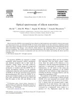
Optical spectroscopy of silicon nanowires
Ngày tải lên :
16/03/2014, 15:06
... Raman scattering spectra of the
SiNWs and crystal silicon. A very sharp and
Fig. 1. A typical SEM image of the morphology of aligned
silicon nanowires of uniform diameter distribution on a silica
substrate.
Fig. ... results on the silica
nanowires [5] that was ascribed to originate from
the oxygen vacancies, while the band peaked at
525 nm is close to the results reported for as-grown
silicon nanowires [6]. According ... crystalline silicon,
and D is the size of crystal. Eq. (1) was used to fit
the Raman spectra. The continuous line in Fig. 3
shows the best-fit result, and the average crystal
size of nanowires D...
- 4
- 365
- 1
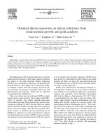
Oriented silicon nanowires on silicon substrates from oxide assisted growth and gold catalysts
Ngày tải lên :
16/03/2014, 15:06
... Oriented silicon nanowires on silicon substrates from
oxide-assisted growth and gold catalysts
Yuan Yao
a
, Fanghua ... 2005
Available online 25 March 2005
Abstract
High-density, oriented silicon nanowires (SiNWs) array were fabricated on (0 0 1) silicon substrates by the oxide-assisted growth
method assisted with ... many unique properties
not found in the bulk materials. Silicon nanowires
(SiNWs) are a particularly important 1D nanomaterial
because silicon is most widely used in electronic indus-
try. Besides...
- 5
- 539
- 0

Polymer assisted synthesis of aligned amorphous silicon nanowires and their core shell structures with au nanoparticles
Ngày tải lên :
16/03/2014, 15:06
... Chemical Physics Letters 397 (2004) 128–132
Polymer-assisted synthesis of aligned amorphous silicon
nanowires and their core/shell structures with Au nanoparticles
Xing-bin Yan
a,b
, Tao Xu
a
, ... Conse-
quently, a great deal of effort has been made in fabricat-
ing Si-based nanostructures, especially silicon nanowires
(SiNWs). Upto now, several methods have been em-
ployed to produce SiNWs, including ... characteristic of a silicon structure, corresponding to
the second-order transverse acoustic phonon mode
(2TA), and the first-order transverse optical phonon
mode (TO) of silicon, respectively....
- 5
- 467
- 0
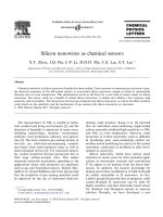
Silicon nanowires as chemical sensors
Ngày tải lên :
16/03/2014, 15:08
... interactions between gas molecules and silicon nanowires, as well as the effect of silicon
oxide sheath on the sensitivity and the mechanisms of gas sensing with silicon nanowires are discussed.
Ó 2003 ... sensitivity of silicon nanowires bundles has been studied. Upon exposure to ammonia gas and water vapor,
the electrical resistance of the HF-etched relative to non-etched silicon nanowires sample ... phenomenon serves as the basis for a new kind of sensor based on silicon
nanowires. The sensor, made by a bundle of etched silicon nanowires, is simple and exhibits a fast response, high
sensitivity...
- 5
- 241
- 1

Silicon nanowires grown on si(1 0 0) substrates via thermal reactions with carbon nanoparticles
Ngày tải lên :
16/03/2014, 15:08
... amount of SiO
2
and C is
S. Botti et al. / Chemical Physics Letters 371 (2003) 394–400 395
Silicon nanowires grown on Si(1 0 0) substrates via
thermal reactions with carbon nanoparticles
S. Botti
a,
*
, ... lm
with strongly reduced SiO
2
content with silicon wires of diameter ranging between 30 and 50 nm decorating the pyramid
walls. The nucleation of the Si nanowires occurs via reduction of the native ... used in similar techniques.
Ó 2003 Elsevier Science B.V. All rights reserved.
1. Introduction
Silicon nanowires with diameter of several tens
of nanometers and length of tens of micrometers,
exhibit...
- 7
- 283
- 0

Temperature dependence of morphology and diameter of silicon nanowires synthesized by laser ablation
Ngày tải lên :
16/03/2014, 15:09
... corresponding
correlation between morphology and diameter of
nanowires. Nanowires of larger diameter (100–150
nm) were inclined to be octopus-shaped, while
nanowires of smaller diameter (10–15 nm) were
inclined ... the
nanowires in this zone is vapor–liquid–solid (VLS)
growth [18]. Energy dispersive spectroscopy (EDS)
analysis indicated that the nanoparticles at the tips
of the nanowires only contained silicon ... the
silicon nanoparticle chains. They proposed that
nucleation and growth occurring alternatively re-
sulted in the formation of chains of silicon nano-
particles. The formation of the kinks of silicon
nanoparticle...
- 5
- 401
- 0

Temperature dependence of the quality of silicon nanowires produced over a titania supported gold catalyt
Ngày tải lên :
16/03/2014, 15:09
... temperature is 500 °C. Silicon nanowires
produced at this temperature have a well-crystal-
lized silicon core with a very thin amorphous sili-
con dioxide outer layer. The length of the
nanowires is in ... (2003) 377–383
and silicon tetrachloride (SiCl
4
). Westwater et al.
[7,8] have reported that the use of silane as Si
source to prepare silicon nanowires via CVD yields
much thinner nanowires than ... silicon nanowires
produced at four different temperatures. Raman spectra of sil-
icon wafer and of the fresh Au/TiO
2
catalyst are also included
for comparison. Lower panel: Raman spectra of silicon...
- 7
- 432
- 0

- bài học quản trị từ silicon valley
- giấy trắng phủ silicon
- tính chất vật lý của silicon
- tính chất hóa học của silicon
- tính chất của silicon
- áo nâng ngực silicon
Tìm thêm:
- hệ việt nam nhật bản và sức hấp dẫn của tiếng nhật tại việt nam
- xác định các mục tiêu của chương trình
- xác định các nguyên tắc biên soạn
- khảo sát các chuẩn giảng dạy tiếng nhật từ góc độ lí thuyết và thực tiễn
- khảo sát chương trình đào tạo của các đơn vị đào tạo tại nhật bản
- khảo sát chương trình đào tạo gắn với các giáo trình cụ thể
- xác định thời lượng học về mặt lí thuyết và thực tế
- tiến hành xây dựng chương trình đào tạo dành cho đối tượng không chuyên ngữ tại việt nam
- điều tra đối với đối tượng giảng viên và đối tượng quản lí
- điều tra với đối tượng sinh viên học tiếng nhật không chuyên ngữ1
- khảo sát thực tế giảng dạy tiếng nhật không chuyên ngữ tại việt nam
- khảo sát các chương trình đào tạo theo những bộ giáo trình tiêu biểu
- nội dung cụ thể cho từng kĩ năng ở từng cấp độ
- xác định mức độ đáp ứng về văn hoá và chuyên môn trong ct
- phát huy những thành tựu công nghệ mới nhất được áp dụng vào công tác dạy và học ngoại ngữ
- mở máy động cơ lồng sóc
- mở máy động cơ rôto dây quấn
- các đặc tính của động cơ điện không đồng bộ
- hệ số công suất cosp fi p2
- đặc tuyến hiệu suất h fi p2