an introduction to objectoriented analysis and design and iterative development by craig larman

an introduction to numerical analysis for electrical and computer engineers - wiley
Ngày tải lên :
31/03/2014, 15:09
... processing, and is an
instance of something called finite impulse response (FIR) filtering. You will
find it useful to note that a
k
= 0fork<0, and k>n,andthatb
j
= 0for
j<0, and j>m. ... added together, there is the possibility that the sum may
not fit in n bits. This is overflow. The condition is easy to detect by monitoring
the signs of the operands and the sum. Suppose that x and ... This is also equivalent to being able to place the elements of A into 1–1
correspondence with the elements of Z.
TLFeBOOK
AN INTRODUCTION TO
NUMERICAL ANALYSIS
FOR ELECTRICAL AND
COMPUTER ENGINEERS
TLFeBOOK
10...
- 605
- 522
- 0


an introduction to information theory- symbols signals and noise - john r. pierce
Ngày tải lên :
11/06/2014, 12:05
... our human nature and activities,
which can be grouped together and understood. Such understanding is an ability to see what
complicated or diverse events really do have in common (the planets ... they
have to prove theorems in order to be certain. Newton himself came to see the importance of proof,
and he proved many new theorems by using the methods of Euclid.
By and large, mathematicians ... production of text (and of spoken
and visual messages as well) is the ergodic source. To understand what an ergodic source is, we
must first understand what a stationary source is, and to explain this...
- 266
- 533
- 0

sea ice an introduction to its physics chemistry biology and geology
Ngày tải lên :
06/07/2014, 15:28
... deep
world ocean, and the transport of natural and anthropogenic substances (tracers)
from the ocean surface to the abyss where these can be stored for centuries. The
latter is of climatic relevance in ... a need to increase our awareness and to expand our research activities
on sea ice in order to answer the many open questions. Increasingly we need to
realize that with the expanding human population ... element in phytoplankton growth, and so contribute to
blooms at the ice edge.
Finally, in Chapter 11, Leanne Armand and Amy Leventer discuss the past
Foreword xi
Contents
Foreword by G.E. (Tony) Fogg...
- 418
- 429
- 0

An Introduction to MEMs Engineering - Nadim Maluf and Kirt Williams Part 1 doc
Ngày tải lên :
10/08/2014, 01:22
... Lacroix and Ken Cioffi of Discera; Michael Cohn of MicroAssem
-
bly; Nelson Fuller of Alumina Micro; and Stephen Durant and Christopher Eide of
Morrison and Foerster. Evan Green and Carter Hand of ... references to each chapter to direct the advanced reader to the source
of the material. We also expanded the glossary to assist the novice in understanding
and relating to a new terminology.
Many people ... products and
developments specific to biochemical analysis and microfluidics. With the emer
-
gence of wireless and radio frequency (RF) as a new market for MEMS technology,
we dedicated Chapter 7 to...
- 20
- 336
- 1

An Introduction to MEMs Engineering - Nadim Maluf and Kirt Williams Part 2 pptx
Ngày tải lên :
10/08/2014, 01:22
... States and sponsored by SPIE of Bellingham, Washington.
•
Micro Total Analysis Systems (µTAS): a conference focusing on microanalyti
-
cal and chemical systems. It is an annual meeting and alternates ... Vector
algebra (using a dot product) shows that the angles between {100} and {110} planes
are 45º or 90º, and the angles between {100} and {111} planes are 54.7º or 125.3º.
Similarly, {111} and ... Informationstechnik GmbH of Teltow, Ger-
many, and is available on-line.
•
Micro/Nano Newsletter: a publication companion to “R&D Magazine”
with news and updates on micromachined devices and nanoscale-level
technologies....
- 20
- 478
- 1
An Introduction to MEMs Engineering - Nadim Maluf and Kirt Williams Part 3 pps
Ngày tải lên :
10/08/2014, 01:22
... lithographie, galvanoformung, und abformung, meaning lithography, elec
-
troplating, and molding.
both PSG and BPSG soften and flow to conform with the underlying surface topog
-
raphy and to improve ... Zorman, C. A., and M. Mehregany, “Materials for Microelectromechanical Systems,” in
The MEMS Handbook, Chapter 15, M. Gad-el-Hak (ed.), Boca Raton, FL: CRC Press,
2002.
[10] Zhang, Z. L., and ... companion material to silicon; the two are bonded
together figuratively and literally in many ways. Silicon originates from processed
and purified silicates (a form of glass), and silicon can...
- 20
- 494
- 1

An Introduction to MEMs Engineering - Nadim Maluf and Kirt Williams Part 4 pptx
Ngày tải lên :
10/08/2014, 01:22
... electronically stored; (b) the alignment marks on the back side of the
wafer are brought in focus; and (c) the position of the wafer is adjusted by translation and rotation
to align the marks to the stored ... transition of the gel to glass and then densification to
silicon dioxide [22]. Silicon nitride, alumina, and piezoelectric PZT can also be
deposited by sol-gel methods.
Electroplating and Molding
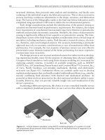
Electroplating ... mask
a
0.707a
54.74°
{100}
{111}
{100}
{111}
Self-limiting
etches
Membrane
<100>
{110}
Figure 3.6 Illustration of the anisotropic etching of cavities in {100}-oriented silicon: (a) cavities,
self-limiting pyramidal and V-shaped pits, and thin membranes; and...
- 20
- 560
- 1
An Introduction to MEMs Engineering - Nadim Maluf and Kirt Williams Part 5 doc
Ngày tải lên :
10/08/2014, 01:22
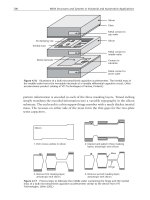
... photoresist and selectively electroplate first metal; (b)
blanket electroplate second metal; and (c) planarize to same thickness.
CHAPTER 4
MEM Structures and Systems in Industrial
and Automotive ... Benecke, and P. Lange, “TMAHW Etchants for Silicon
Micromachining,” Proc. 1991 Int. Conf. on Solid-State Sensors and Actuators, San Fran-
cisco, CA, June 24–27, 1991, pp. 815–818.
[9] Ammar, E. S., and ... another approach to release crystalline microstructures. Standard lithography
and etching methods define trenches between 10 and 50 µm in depth, which are then
coated on the top, sidewalls, and...
- 20
- 564
- 4


Tài liệu AN INTRODUCTION TO THE ANALYSIS OF ALGORITHMS pdf
Ngày tải lên :
19/02/2014, 20:20
... the
average and standard deviation ordinarily allows us to predict performance
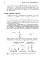
Figure 1.3
2NlnN − .846N
Distributions for compares in quicksort, ≤ N ≤
(scaled and translated to center and separate ... precise
that they can be used to accurately predict performance and to compare algo-
rithms, and able to be rened, in principle, to the precision needed for the
application at hand. Such techniques ... be many opportunities to honor Philippe in
the future and expect to be fully and personally involved on these occasions.
Brilliant, creative, inquisitive, and indefatigable, yet generous and...
- 593
- 4.2K
- 0
Tìm thêm:
- hệ việt nam nhật bản và sức hấp dẫn của tiếng nhật tại việt nam
- xác định các mục tiêu của chương trình
- xác định các nguyên tắc biên soạn
- khảo sát các chuẩn giảng dạy tiếng nhật từ góc độ lí thuyết và thực tiễn
- khảo sát chương trình đào tạo của các đơn vị đào tạo tại nhật bản
- khảo sát chương trình đào tạo gắn với các giáo trình cụ thể
- xác định thời lượng học về mặt lí thuyết và thực tế
- tiến hành xây dựng chương trình đào tạo dành cho đối tượng không chuyên ngữ tại việt nam
- điều tra đối với đối tượng giảng viên và đối tượng quản lí
- điều tra với đối tượng sinh viên học tiếng nhật không chuyên ngữ1
- khảo sát thực tế giảng dạy tiếng nhật không chuyên ngữ tại việt nam
- khảo sát các chương trình đào tạo theo những bộ giáo trình tiêu biểu
- nội dung cụ thể cho từng kĩ năng ở từng cấp độ
- xác định mức độ đáp ứng về văn hoá và chuyên môn trong ct
- phát huy những thành tựu công nghệ mới nhất được áp dụng vào công tác dạy và học ngoại ngữ
- mở máy động cơ lồng sóc
- mở máy động cơ rôto dây quấn
- các đặc tính của động cơ điện không đồng bộ
- hệ số công suất cosp fi p2
- đặc tuyến hiệu suất h fi p2